

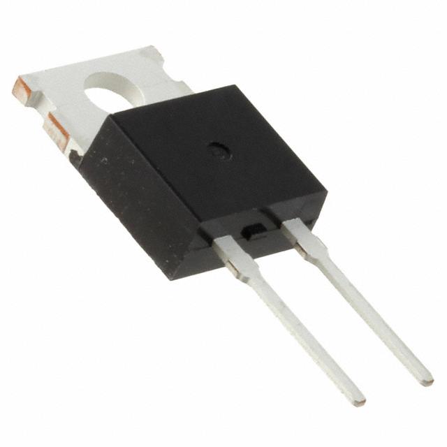
Description
Maximum Continuous Drain Current: 10.6 A
Transistor Material: Si
Width: 6mm
Transistor Configuration: Single
Maximum Drain Source Voltage: 60 V
Package Type: MLP
Number of Elements per Chip: 1
Minimum Gate Threshold Voltage: 2V
Maximum Operating Temperature: +150 °C
Typical Gate Charge @ Vgs: 32 nC @ 10 V
Channel Type: N
Length: 5mm
Pin Count: 8 Channel Mode: Enhancement Mounting Type: Surface Mount Maximum Power Dissipation: 2.5 W Series: UltraFET Maximum Gate Source Voltage: -20 V, +20 V Height: 0.75mm Minimum Operating Temperature: -55 °C Maximum Drain Source Resistance: 12 mΩ Manufacturer Standard Lead Time: 29 Weeks Detailed Description: N-Channel 60V 10.6A (Ta), 22A (Tc) 2.5W (Ta), 78W (Tc) Surface Mount 8-MLP (5×6), Power56 Vgs(th) (Max) @ Id: 4V @ 250µA Operating Temperature: -55°C ~ 150°C (TJ) Package / Case: 8-PowerWDFN Base Part Number: FDMS56 Gate Charge (Qg) (Max) @ Vgs: 45nC @ 10V Rds On (Max) @ Id, Vgs: 11.5mOhm @ 10.6A, 10V FET Type: N-Channel Manufacturer: ON Semiconductor Drain to Source Voltage (Vdss): 60V Vgs (Max): ±20V Input Capacitance (Ciss) (Max) @ Vds: 2800pF @ 30V Mounting Type: Surface Mount Series: UltraFET™ Supplier Device Package: 8-MLP (5×6), Power56 Drive Voltage (Max Rds On, Min Rds On): 6V, 10V Packaging: Cut Tape (CT) Current – Continuous Drain (Id) @ 25°C: 10.6A (Ta), 22A (Tc) Customer Reference: Power Dissipation (Max): 2.5W (Ta), 78W (Tc) Technology: MOSFET (Metal Oxide)
This ismanufactured by ON Semiconductor. The manufacturer part number is FDMS5672. While 10.6 a of maximum continuous drain current. The transistor is manufactured from highly durable si material. Furthermore, the product is 6mm wide. The product offers single transistor configuration. It has a maximum of 60 v drain source voltage. The package is a sort of mlp. It consists of 1 elements per chip. Whereas its minimum gate threshold voltage includes 2v. It has a maximum operating temperature of +150 °c. With a typical gate charge at Vgs includes 32 nc @ 10 v. The product is available in [Cannel Type] channel. Its accurate length is 5mm. It contains 8 pins. The product carries enhancement channel mode. The product is available in surface mount configuration. Provides up to 2.5 w maximum power dissipation. The product ultrafet, is a highly preferred choice for users. It features a maximum gate source voltage of -20 v, +20 v. In addition, the height is 0.75mm. Whereas, the minimum operating temperature of the product is -55 °c. It provides up to 12 mω maximum drain source resistance. It has typical 29 weeks of manufacturer standard lead time. It features n-channel 60v 10.6a (ta), 22a (tc) 2.5w (ta), 78w (tc) surface mount 8-mlp (5×6), power56. The typical Vgs (th) (max) of the product is 4v @ 250µa. The product has -55°c ~ 150°c (tj) operating temperature range. Moreover, the product comes in 8-powerwdfn. Base Part Number: fdms56. The maximum gate charge and given voltages include 45nc @ 10v. It has a maximum Rds On and voltage of 11.5mohm @ 10.6a, 10v. It carries FET type n-channel. The on semiconductor’s product offers user-desired applications. The product has a 60v drain to source voltage. The maximum Vgs rate is ±20v. The product’s input capacitance at maximum includes 2800pf @ 30v. The product ultrafet™, is a highly preferred choice for users. 8-mlp (5×6), power56 is the supplier device package value. The minimum and maximum Rds On drive voltage includes [Drive Voltage (Max Rds On, Min Rds On)]. In addition, cut tape (ct) is the available packaging type of the product. The continuous current drain at 25°C is 10.6a (ta), 22a (tc). The product carries maximum power dissipation 2.5w (ta), 78w (tc). This product use mosfet (metal oxide) technology.

Reviews
There are no reviews yet.